Read Appendix B.1
Today's News: October 8
You should have gotten your exam back.
Examples:
B.1: Introduction
- Main memory is usually made from dynamic ram (DRAM) which has a typical access time of 30 ns or more.
- In the 5-stage pipeline we assume that an instruction fetch or a memory read can be done in one cycle.
- One cycle is typically a fraction of a nanosecond.
- It does not make sense to stall for 50 to 100 cycles each time we do an instruction fetch.
- This problem is solved by using a cache, a relatively small fast memory that holds a subset of the contents of the main memory.
- Assume we have a cache that can be accessed in one cycle.
When an access is attempted:- first look in the cache
- if there, we are done. This is called a cache hit.
- if not, we look in main memory. This is called a cache miss.
- The number of extra cycles needed during a cache miss is called the miss penalty.
- The fraction of time that an access is found in the cache is called the cache hit ratio.
- The fraction of time that an access is not found in the cache is called the cache miss ratio.
Suppose a cache can be accessed in one cycle, the hit ratio is 97%, and the miss penalty is 30 cycles.
What is the average number of cycles needed for an instruction fetch?
Solution:
What is the average number of cycles needed for an instruction fetch?
Solution:
Note that the miss penalty is the number of extra cycles required on a miss.
.97 × 1 + .03 × 31 = .97 + .93 = 1.90 cycles or:
1 + .03 × 30 = 1 + .9 = 1.9 cycles.
.97 × 1 + .03 × 31 = .97 + .93 = 1.90 cycles or:
1 + .03 × 30 = 1 + .9 = 1.9 cycles.
ClassQue: Cache Terminology
Memory Hierarchy
- The fastest memory of a computer system is the registers.
- Compilers try to keep as much data in registers to avoid memory accesses.
- If memory accesses cannot be satisfied in the cache, main memory must be accessed.
- If there is not enough main memory, some data will need to be stored on disk.
- Modern computers have several levels of cache between the registers and main memory.
| Level | 1 | 2 | 3 | 4 |
| Name | Registers | Cache | Main Memory | Disk |
| Typical Size | < 1KB | 32KB - 8MB | < 512GB | > 1 TB |
| Technology | custom, multiple ports | on-chip CMOS SRAM | CMOS DRAM | Magnetic disk |
| Access time (ns) | 0.15-0.30 | 0.5 - 15 | 30-200 | 5,000,000 |
| Bandwidth (MB/sec) | 100,000 - 1,000,000 | 10,000 - 40,000 | 5000 - 20,000 | 50-500 |
| Managed by | Compiler | Hardware | OS | OS, user |
Example:
Suppose it takes 30 ns to access one byte. What is the bandwidth in MB/sec?
Solution:
Solution:
30 ns to access a byte means 1 byte every 30 ns = 1 byte every 3 × 10⁻⁸ seconds
for a bandwidth of 1/(3 × 10-8) bytes per second = 3.3 × 107 bytes/sec. = 33 MB/sec.
- Main memory and disks are organized so that after a latency, a block can be transferred quickly.
- When a cache miss occurs, a block is transfered to the cache.
- Temporal locality: the same data is likely to be needed again soon.
- Spatial locality: data near recently accessed data will be needed soon.
- The miss penalty depends on both the latency and the bandwidth.
- With in-order execution, a cache miss causes the pipeline to stall.
- With out-of-order execution, a stall of subsequent instructions might not be necessary.
ClassQue: Memory Accesses per Instruction
Example: (Similar to the example on page B-5 of the text)
Suppose we have the standard MIPS 5-stage pipeline which has a CPI of 1 when all memory accesses are cache hits.
Loads and stores are 25% of all instructions, the miss rate is 4% and the miss penalty is 20 cycles.
How much faster would the computer be with no cache misses?
Incorrect Solution:
Loads and stores are 25% of all instructions, the miss rate is 4% and the miss penalty is 20 cycles.
How much faster would the computer be with no cache misses?
Incorrect Solution:
The CPI with cache misses is 1 + .25 × .04 × 20 = 1 + .20 = 1.20, so it would be 1.20 times as fast or 20% faster.
Correct Solution:
CPI with cache misses is 1 + 1.25 × .04 × 20 = 1 + 1.0 = 2.0, so it would be 2 times as fast or 100% faster.
A direct mapped cache example
- Suppose we have a cache block size of 64 bytes and a cache with 256 blocks.
- The size of the cache is 64 × 256 = 16K.
- A memory address looks like this:
--------------------------------- | tag | index | offset | --------------------------------- 8 bits 6 bits - The offset is the offset into the cache block.
- The index determines where in the cache the block will be stored.
- If a memory address is 32 bits, the tag is 32 - 8 - 6 bits = 18 bits.
- A cache block looks like this:
--------------------------------- | tag | data | --------------------------------- 18 bits 64 bytes - We need to store the tag with the data since several different memory addresses will correspond to the same cache entry.
- We also need one valid bit to indicate that the entry contains valid data (not shown).
- If the memory address is 0x23456, what is the index and what is the tag?
- We need to write the address in binary: 0000 0000 0000 0010 0011 0100 0101 0110
- We can rewrite this as: 000000000000001000 11010001 010110
- The low 6 bits are the offset: 010110 = 0x16.
- The next 8 bits is the index: 11010001 = 0xd1
- The rest is the tag: 000000000000001000 = 00 0000 0000 0000 0100 = 0x8
- To look up the byte with address 0x23456 in the cache:
- find the entry at index 0xd1
- if the valid bit is clear, the data is not in the cache.
- otherwise, compare the tag in the entry to the tag of this address
- if they match, the data is in the cache
- The byte at the address 0x33456 will be stored in the same cache location.
ClassQue: Direct Mapped Cache Location
The above is an example of a direct mapped cache.
Given an address, you can tell exactly where in the cache it would be stored.
Why not just put a cache block anywhere in the cache?
It might take too long to do the lookup.
Today's News: October 10
No news yet.
Examples:
Four Questions on Cache Design
- block placement: Where can a block be stored in the cache?
- block identification: How is a block located in the cache?
- block replacement: What block should be replaced on a miss?
- write strategy: What happens on a write?
Block Placement
- The simplest method is the direct mapped cache:
- Given an address it can only be in one position in the cache.
- The mapping is given by:
block position = (Block Address) MOD (Number of blocks in the cache) - Note that the Block Address is the address with the offset bits removed.
- Note that the block position is just the index.
- If a block can be placed anywhere in the cache, the cache is called fully associative
- If a block is be restricted to a set of places in the cache, the cache is called set associative
- A set is a group of blocks in the cache.
- If there are n blocks in a set, the cache is called n-way set associative
- The larger the value of n, the more hardware is necessary to do a fast lookup.
- A block is mapped into a set, but then can be placed anywhere in the set.
- Usual mapping is called bit selection:
block position = (Block Address) MOD (Number of sets in the cache)
- A fully associative cache with m blocks is m-way set associative.
- Most real caches are direct mapped, 2-way set associative, or 4-way set associative.
ClassQue: Cache Block Placement 1
Block identification
There are 2 parts to this:
Find out where it might be
Check all of these possible locations
Check all of these possible locations
- Each block of the cache has a valid bit indicting whether the data in that block of the cache is valid
- Each block of the cache has a tag which contains most of the address of the starting block
- Figure B.3 below shows the format of an address.
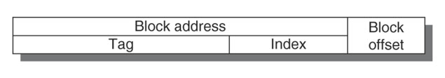
- Don't need to check the offset since the entire block is in the cache
- Checking the index is redundant since it determines which set the data can be in.
- Only need to store the tag.
- Figure B.2 shows an example of a cache with 8 blocks.
ClassQue: Cache Block Identification 1
Block replacement
This is not an issue for direct mapped caches, since there is no choice.The standard methods are:
- random: actually pseudorandom for reproducibility
- least recently used (LRU): reduces the chance of replacing a block that will be used often.
This requires the most hardware which grows exponentially with the number of choices.
Sometimes an approximation is used. - First in, first out (FIFO): requires less hardware than LRU.
Today's News: October 15
No news yet.
Write strategy
- No change to the cache or memory is necessary during a read hit.
- Reads are the common case in cache accesses.
- Each instruction requires a read during the instruction fetch.
- Usually separate caches are used for instruction and data access (loads and stores).
- Even among data accesses, loads are typically more than twice as common as stores.
- write-through: information is written both to the cache and the (lower-level) memory.
Easier to implement than write-back, especially for multiprocessors.
Can cause a write stall while waiting for write to memory to complete. - write-back: information is written only to the cache.
The lower-level memory is only updated during replacement.
Requires use of a dirty bit.
Requires less memory bandwidth than write-through and can use block transfers.
A read miss might require a write to memory.
- write allocate: fill the cache with the required data, as done with a read miss.
- no-write allocate: never fill the cache on a write miss.
Example:
Suppose addresses are 40 bits, the cache is 64K and uses 64-byte blocks with 2-way set associative placement.
What is the format of a memory address? That is, which bits are used for the tag, index, block address, and offset?
Also, what is the maximum number of gigabytes this processor can access?
Solution:
What is the format of a memory address? That is, which bits are used for the tag, index, block address, and offset?
Also, what is the maximum number of gigabytes this processor can access?
Solution:
The address is 40 bits. 64 = 26 so the block offset is 6 bits.
The index indicates which set to use. There are 64K/64 = 1K blocks with 2 blocks per set, or 512 = 29 sets. The index is 9 bits.
The remainder: 40 - 9 - 6 = 25 bits are for the tag.
The block address is the tag and the index.
The maximum number of gigabytes that can be accessed is 240/230 = 1K gigabytes, (or twice this).
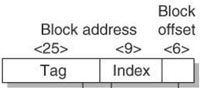
The Opteron data cache
The AMD Opteron uses 40-bit addresses with a 64K data cache.The cache has 64-byte blocks with 2-way set associative placement.
It uses LRU replacement, write-back and write-allocate on a write miss.
It is shown in Figure B.05
The numbers show the steps that occur on a cache hit for a 64-bit memory access.
- The (physical) address is determined. (Details in Section B.4.)
- The index selects the two cache entries of the corresponding set.
- The tag in each cache block is compared to the tag of the memory address (if the valid bit is set).
- The upper 3 bits of the block offset are used to specify an 8-byte portion of the matched block.
For a hit:
- If this is a read, the data is transfered from the cache.
- If this is a write, the data is written to the cache. Since write-back is used, the memory does not need to be accessed during a hit.
Since this uses write-back, if its dirty bit is set, the entire block is written back to memory through the victim buffer.- On a read, the entire block is read and stored in the cache while an 8-byte part is returned to the CPU.
- On a write, the entire block is read and stored in the cache (write-allocate) and then the 8-byte value is written to the cache and the dirty bit is set.
ClassQue: Figure B.5 Questions 1